Data storage in NAND flash memory is a complex process that is not only difficult to understand, but also challenging to explain. Humans are good at abstraction, and we use this skill to enhance technology, even if we are not aware of what is exactly going on at the level of matter. In the case of NAND flash, we understand it on different levels. We start from the most basic unit of memory, the memory cell whether floating gate or charge trap, and then we dig deeper. We then get into the chemical structure and go down to the atomic level. It is an interesting technology. Scientists and Engineers have done an unimaginable job of using electric charge to store data inside these nanoscopic cells. Are we confused yet? Don’t be… this will all fall into place.
When we employ NAND flash in practical applications, like SSDs for instance, there is much to examine. One of the most common ideas is that of storage density. Storage density determines how many bits of data can be stored inside a single memory cell. In our first article of ‘Learning to Run with Flash 2.0’ , we examine and try to provide somewhat of a basic understanding of NAND types, along with the give and take of each.

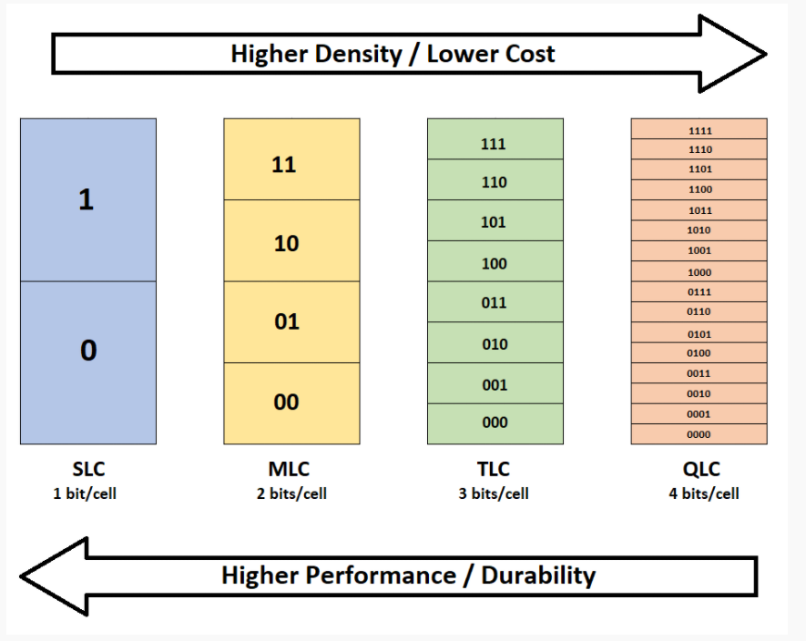
On the basis of storage density, NAND flash is available in four types. These are SLC (Single-Level Cell), MLC (Multi-Level Cell), TLC (Triple-Level Cell), and QLC (Quad-Level Cell). Penta-Level Cell is already in development, but for now, we have these four to talk about.
WHAT IS A MEMORY CELL IN NAND FLASH?
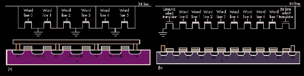
NAND flash is a non-volatile memory, but the term “memory” is technically incorrect. In this memory, the data is still present and intact, even if the input power is cut. However, we traditionally call it a memory cell, and there is no harm in that. How a memory cell stores the data is a very interesting phenomenon of physics. The memory cell is made up of a transistor. Traditionally, it was a floating-gate transistor but modern SSDs utilize charge-trap flash, which can be considered a modern variant of the same technology. It just has better charge-holding and hence data retention capabilities.
So, we have a memory cell made up of a transistor, and it can hold a very small amount of charge inside two layers of insulator material. If you understand the normal transistor , you would know that it can work as a switch. Two terminals can allow or disallow the flow of current depending on the status (On/Off) of the third terminal, called a gate. The voltage (threshold) at which the transistor opens or closes is fixed and can’t be changed. {n the case of a floating gate transistor, some more layers are added, and it changes the threshold voltage. This change happens due to the charge that is stored between those insulating materials (called the floating gate in FGMOS). Different levels of charge on the floating gate pose different variations in the threshold voltage.
The controller on your SSD has many roles, but one of its fundamental roles is to detect this threshold voltage or a change in it. For example, it could be programmed to detect “0” when the threshold voltage is higher or “1” when the voltage is lower.
When we combine literally billions of these cells, we can create a huge array of cells that can store a very large number of these 0s and 1s. These 0s and 1s are better known as…data. Let’s take a look at each cell type, as we might identify them with SSDs, and examine the good…and not so good of each.
#1 – SLC (SINGLE LEVEL CELL)
SLC has the most basic type of design among all NAND flash types. One cell can hold either 0 or 1, and in result, is the fastest and most reliable of all types. Consider this as a switch, off or on. It is also the most expensive because it doesn’t utilize the full capabilities that each memory cell has. It is reserved exclusively for enterprise SSDs due to the high cost and continuous operation capabilities. We do see SLC used as SLC cache in some client SSDs while, TLC or QLC have become primary storage medium today.
This photo is one of our first of SLC NAND and taken by Paul Alcorn for his report way back in 14 March 2012. It is of the Toshiba MK4001GRZB 400GB SAS 6Gb/s Enterprise SLC SSD.
SLC NAND flash is reserved for data centers, servers, and other types of enterprise storage, not because of the performance but because of the higher endurance as well. SLC NAND flash offers an exceptional endurance ranging from 50,000 to 100,000 Program/Erase cycles.
If we look at the design, SLC has only two discrete voltage levels, i.e., high/low or 0/1. A single memory cell can have one of these two states, and it either represents a bit value of 0 or 1. To store and retrieve the data, very basic algorithms are required in the controller. Wear-leveling, garbage collection, and TRIM are much easier to implement.
WHY DON’T WE SEE SLC NAND IN SSDS TODAY?
The first REASON is the cost. aS SLC nand is THE most expensive per GB, it is not cost-effective for large-scale consumer storage applications. The second trade-off is the lower capacity on the same chip size compared to other types of NAND flash. slc nand is used widely in enterprise, aerospace, industrial, and defense applications. So, it is hardly available for other applications.
#2 – MLC (MULTI-LEVEL CELL)
As we had explained above, SLC has the simplest design because a single memory cell is used to store one bit of data. With MLC, the complexity increases as now, a single cell is used to hold two bits of data. The number of discrete voltage levels increases. Instead of either high or low voltage, the cell will have two more levels in between. In terms of bit values, it can have one of the four unique bit combinations, i.e., 00, 01, 10, or 11. The storage density increases by 100% but the physical footprint remains the same.
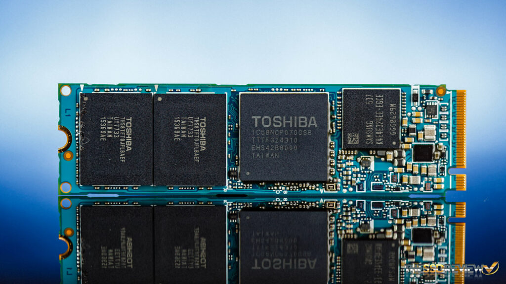
This photo depicts Toshiba MLC memory in the OCZ RD400 from our report on 24 May 2016.
MLC NAND flash is typically reserved for enterprise SSDs as the 3D stacking in TLC and QLC offers almost similar endurance and performance at a lower cost. This was available in older consumer SSDs like Samsung 970 Pro, Toshiba OCZ RD400, and Samsung 860 Pro, but today, it is rare to see. If we talk about endurance, MLC can offer 3,000–10,000 Program/Erase cycles. The number decreased because of the increased wear on the cell and the complexity of handling that data.
SO WHY NO MLC NAND IN SSDS TODAY?
With increased storage density, we trade off the endurance significantly compared to SLC. MLC NAND flash is slower than SLC, error rates are higher, and its high cost to manufacture limits consumer production.
#3 – TLC (TRIPLE LEVEL CELL)
Triple-Level Cell can store 3 bits of data per cell. This means we have 8 possible voltage levels. From MLC, the storage density is increased by 50% and 200% from SLC. This increased storage space is generally considered a good compromise between the SLC’s high endurance but high cost and QLC’s low endurance and low cost. Generally, TLC NAND flash has endurance between 1,000 – 3,000 Program/Erase cycles. To manage this low inherited endurance, manufacturers rely on DRAM cache, TRIM, garbage collection, write cache, and various other methods.
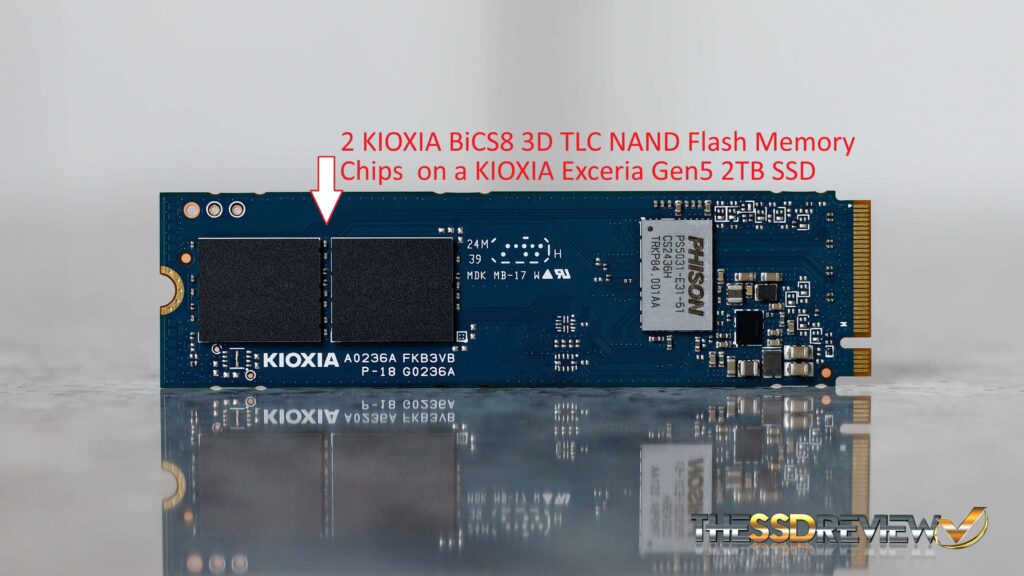
TLC is mainly used in consumer SSDs as MLC has become obsolete in the client market. With the help of 3D stacking, it can be scaled significantly and still offer good reliability. To improve its raw performance, especially in write scenarios, manufacturers generally employ a pseudo-SLC cache where the same TLC cells are used in SLC mode.
This photo is from one of our latest reports on the Lexar 1090 pro Gen5 2TB SSD which uses Longsys branded Micron’s 232-layer 3D TLC B58r Fortis Flash NAND flash memory.
TLC NAND FLASH TRADE-OFF
For the increased storage density and lower cost-per-GB, we trade off the endurance. there are also more errors and higher write amplification. Because a single cell is being overused compared to SLC and MLC, TLC has a lower lifespan as well. Slower write speed is yet another drawback because of the higher number of precise voltage levels inside a single memory cell.
#4 – QLC (QUAD LEVEL CELL)
Until now, QLC has demonstrated the highest level of storage density among all types of NAND flash. A single cell can hold four bits of data with the 14 different possible voltage levels. You can imagine the level of complexity and the software refinements, like ECC, required to handle errors. In QLC, the storage density increases by 33x from MLC and 4x that of SLC. To maintain data integrity, LDPC (Low-Density Parity-Check) is a must. An even heavier and larger SLC write cache is employed to compensate for the extremely low raw write speed. QLC generally has endurance of 100-1000 Program/Erase cycles.
QLC is used heavily in consumer environments where storage density at lower prices is the priority. Another major use that has emerged is with AI training, where data integrity isn’t as important as the size of the datasets. QLC SSDs help a lot in saving budgets for AI data and training companies.
WHY ISN’T QLC MORE COMMON IN SSDS?
In exchange for the highest storage density and lowest cost per GB, we get a major disadvantage of reduced endurance and lifespan. Because a single memory cell is used to hold 4 bits of data, the write performance is very low, mainly due to the precision required to maintain that short voltage window. All in all, QLC NAND flash is preferred where storage space is prioritized over reliability.
FINAL THOUGHTS… AND A BIT OF A REQUEST
This is our first article in our new series “Learning to Run with Flash 2.0”. It would be very beneficial if readers shared their feedback or suggestions in the comments, as this would assist in our direction for future posts. Constructive criticism is always welcome. Our plan is to cover a wide array of SSD topics. If you want us to cover anything specifically, we are waiting for your words.
Thank you for reading!
This is the first article of we hope to be many from our newest addition at The SSD Review, Anshul Rana. Anshul has a B.E in Electronics and Communication Engineering and also has his own website at www.storedbits.com. Amazing Work Anshul and Welcome to TSSDR!